What the measurements would build.
Concepts drawn from our numbers. Designs, not products: nothing here exists in hardware, and every claim says what would have to be measured for it to hold.
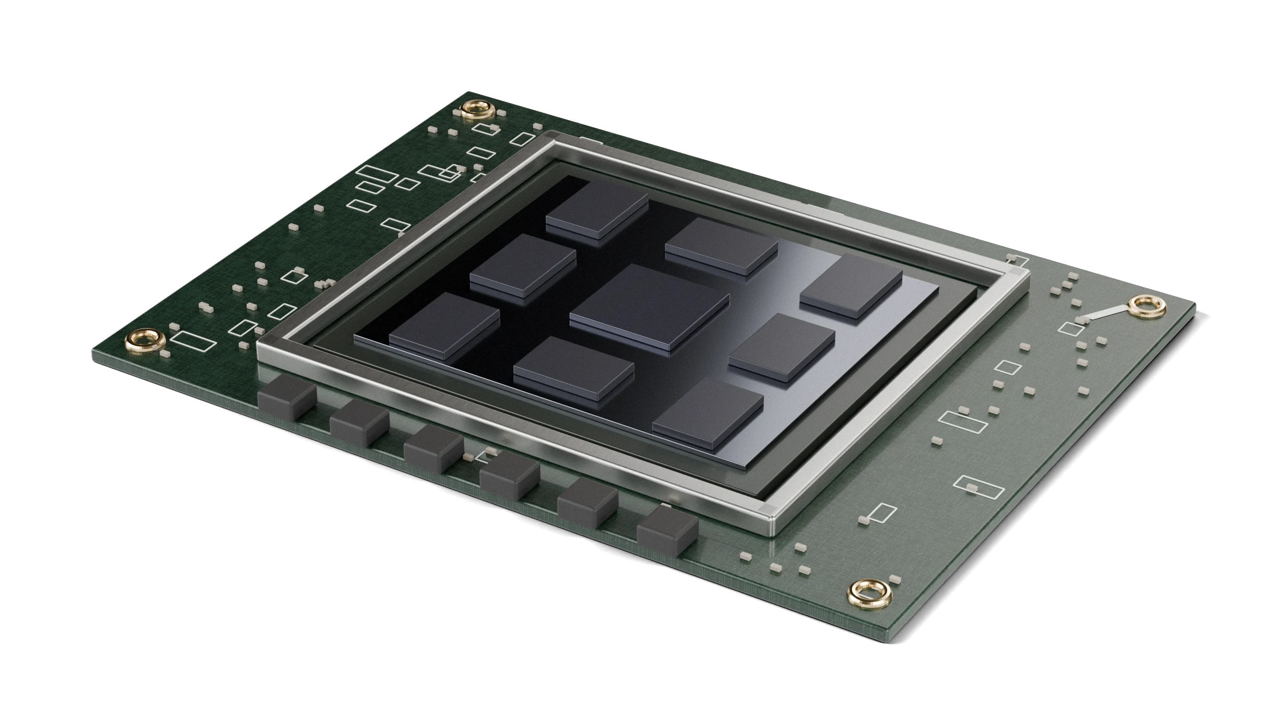
A decode-first module.
Decode reads every weight and every cached token once per step and does little arithmetic on them. The part that serves it well is memory first: a small compute die in the middle of a ring of eight memory stacks, on one interposer. The ring sets the footprint, not the die.
Sized to its bandwidth
The die is only as large as the memory can feed, and it runs at a capped clock by design. On the AMD Ryzen AI Max+ 395, capping the shader clock at 1,800 MHz cut 7B decode energy per token 37% at 4% less speed. A decode part lives there permanently, so its power stage row is short and its cooling is a flat vapour-chamber plate rather than a fin stack.
Paid for by the batch
Eight requests at once cut energy per token by 72% on one chip. The module is meant to run eight or more sequences per step, always, and the sled's scheduler keeps it there.
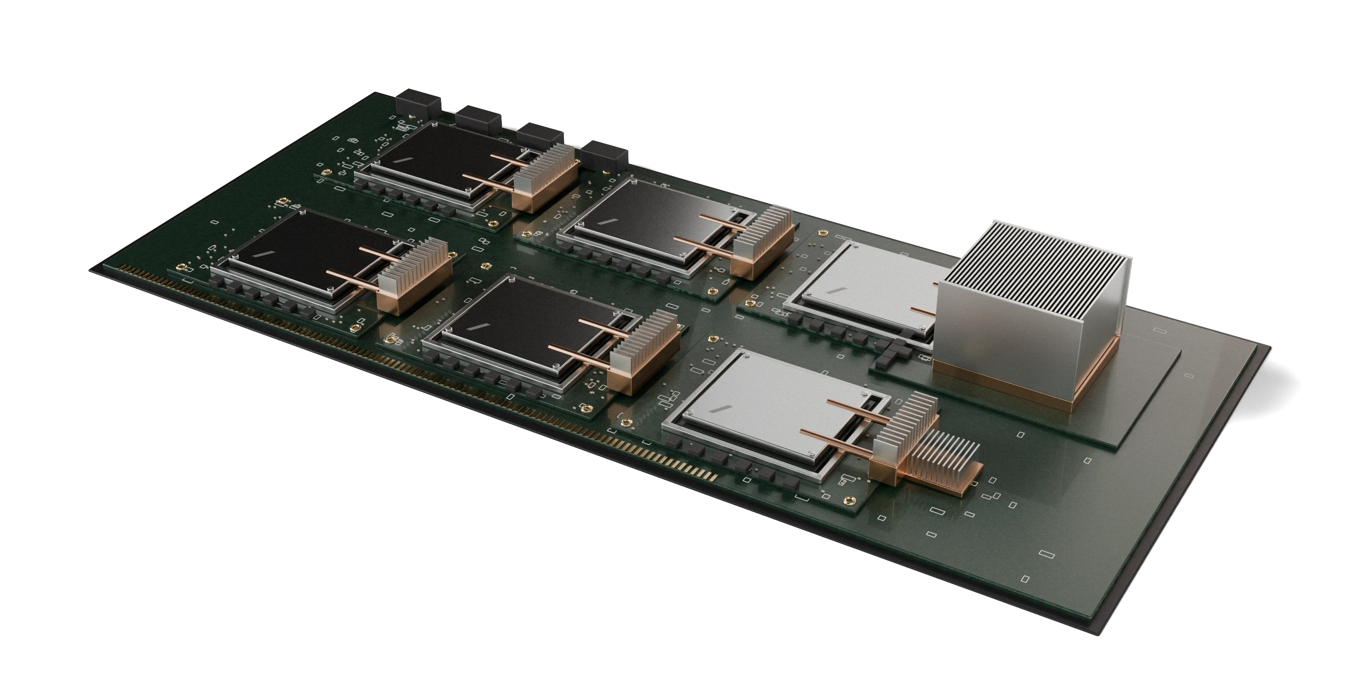
A sled that splits prefill from decode.
Prefill is compute bound; a prompt token costs about a fortieth of a generated one. Putting both on one die buys compute that idles during decode and bandwidth that idles during prefill. The sled puts six decode modules behind one compute-dense prefill module with a tall heat sink, and a switch between them, so the cache handoff stays on one board.
One prefill, one life
A request is prefilled once on the front module and its cache handed to a decode module, where it lives for the rest of the request. A prefix cache hit skips the front module entirely.
What would have to be true
Joules per correct answer at eight slots under a cap, below the single-chip figure by the idle and prefill share it no longer carries. The cache transfer hidden under decode time up to the prompt length where the board link saturates. Six capped modules idling for less than one chip at 17 to 26 W. None of these are measured yet; the Systems page is where the measured recipe lives, and the plan for measuring these is in the research repository.
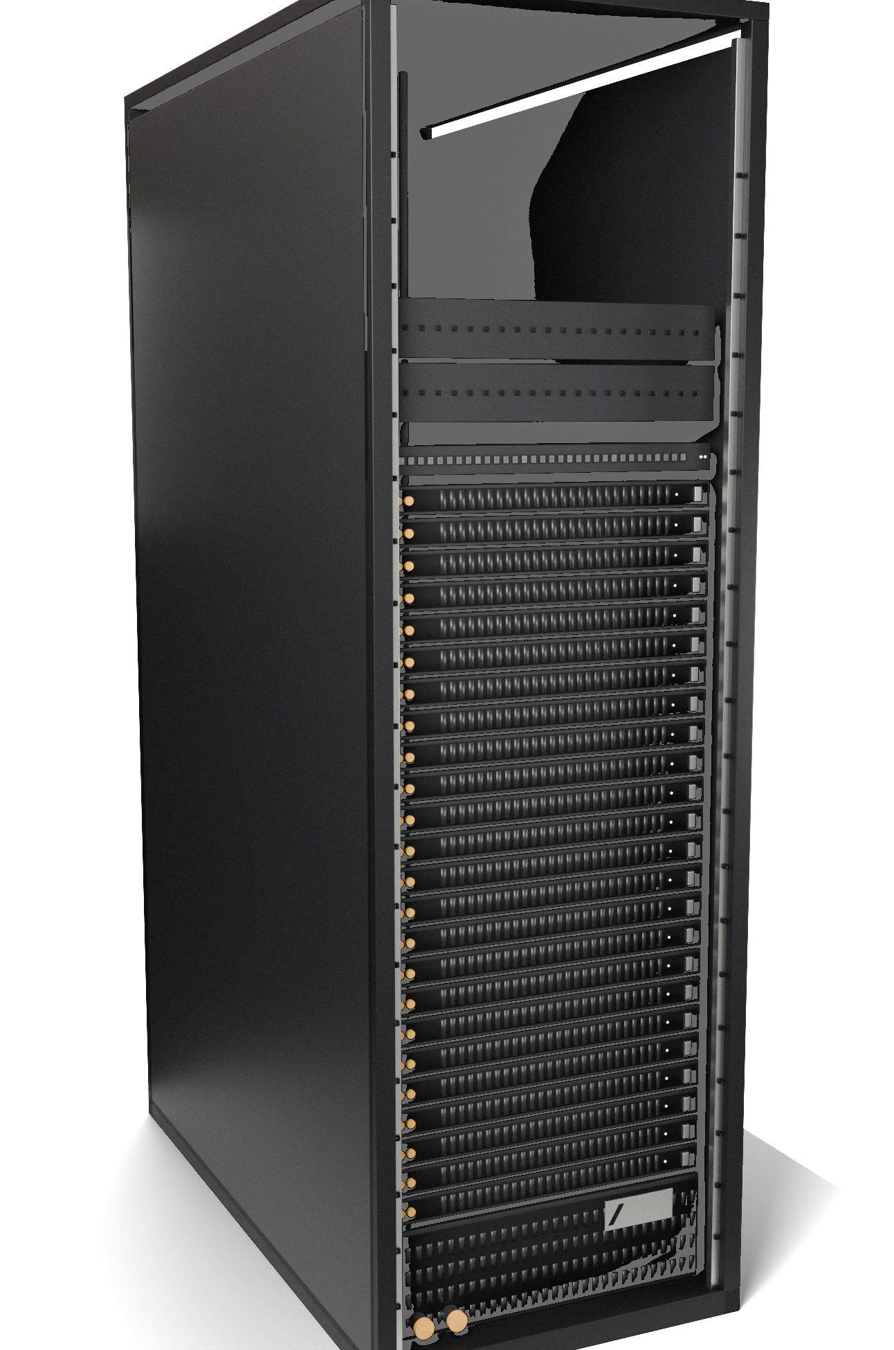
A rack built around the sled.
Twenty-four sleds, a coolant distribution unit in the bottom four units, a switch at the top, and a vertical busbar at the rear so no sled carries its own power supply. Every sled face has two quick-disconnect couplers on the left, because the cold plates on the decode modules are liquid cooled from the start; there is no air path through the module and no fan in the sled.
Why liquid, why a busbar
A capped decode module draws a fraction of a conventional accelerator's power, so the rack's heat is modest for its density; what liquid buys is a flat cold plate and a 1U sled, which is what keeps twenty-four of them in one cabinet. The busbar removes twenty-four power supplies and their conversion losses from the rack, the overhead that sits between chip energy and wall energy in every measurement we have made.
What would have to be true
The idle floor of a full rack at low load, measured at the wall, has to stay below the sum of its parts idling; the coolant unit's pumps have to cost less than the fans they replace; and the switch has to carry cache handoffs between sleds within the time decode hides them. The two-box microbenchmark in our cluster groundwork is the first of those to run.
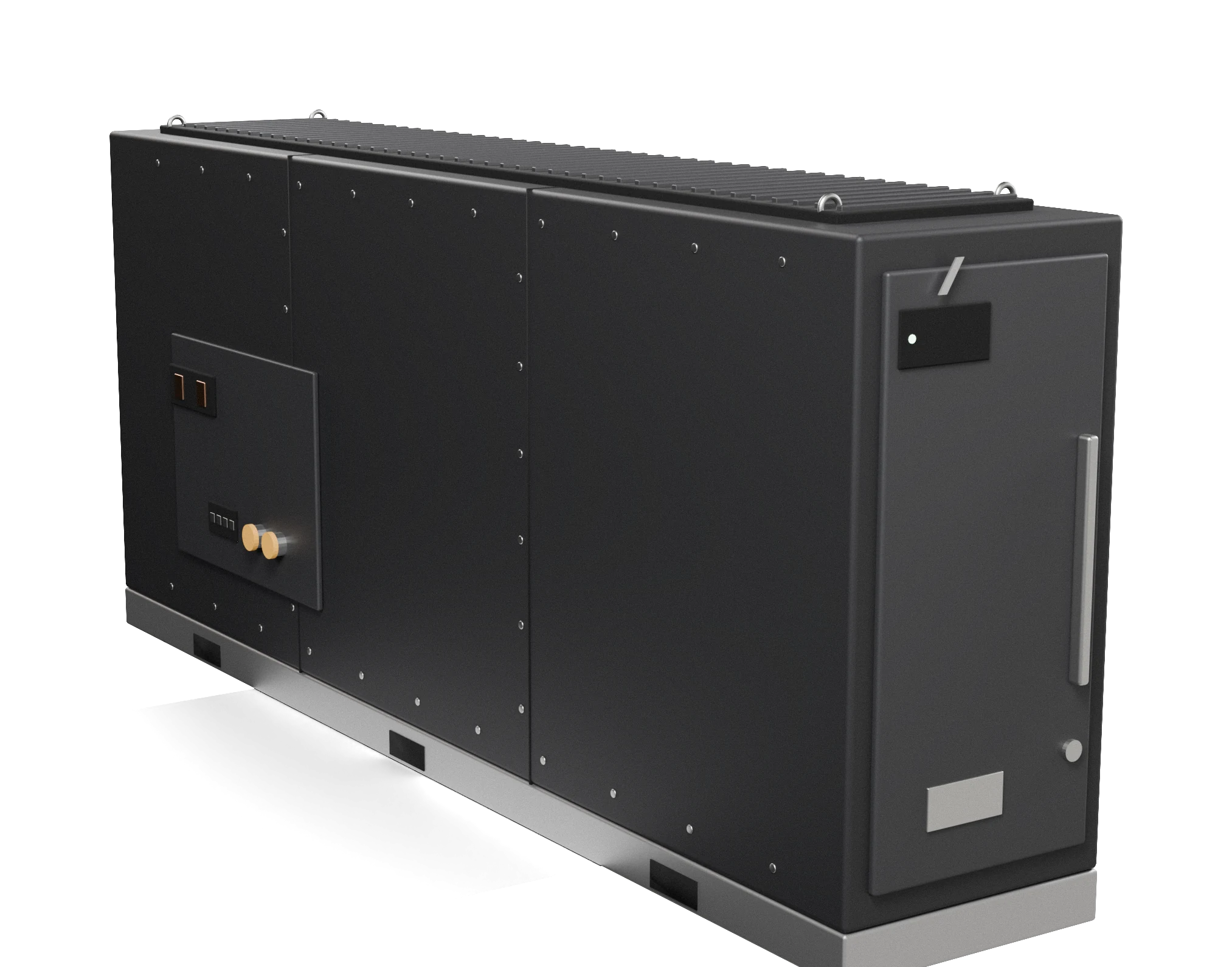
A cell that is a datacenter on its own.
A low, narrow, deep block, 0.6 by 1.2 by 3.0 metres, the proportions of an accelerator card lying flat and stretched back. Decode sleds load from the narrow front in one column and run the depth of the cell; heat leaves through a louvred band along the whole top, fed by the sleds' liquid loop. Alone, it needs only power and a network drop. Each long side is a blind-mate dock with two coolant couplers, a fibre plate and a busbar cover, so a second cell pushed against the first connects without anyone opening either.
Alone, or a hundred in a row
Docked side by side, the coolant trunk, the busbar and the fibre pass through every cell: a row takes power at one end, rejects heat along its whole top, and its switches form one fabric. A row of a hundred is one unit to the scheduler and a hundred units to the forklift. Pull one out and its neighbours' docks close.
Why one is cheap, and the hundredth cheaper
The sleds spend their silicon on commodity stacked memory rather than a large die and run capped, which leaves out the expensive part of an accelerator. No power supply per cell, no raised floor, no chilled-water plant, no building: the cell is its own room. One enclosure, one door, one dock, built in volume. We have not costed it and will not print a price until a bill of materials exists.
What would have to be true
The top band rejects a full cell's heat at the design ambient without a chiller, at a fan power that keeps wall energy per correct answer below the single-chip figure. The couplers hold pressure through a hundred dockings. The busbar carries a row's current and a cell can be pulled live. None of these are measured.
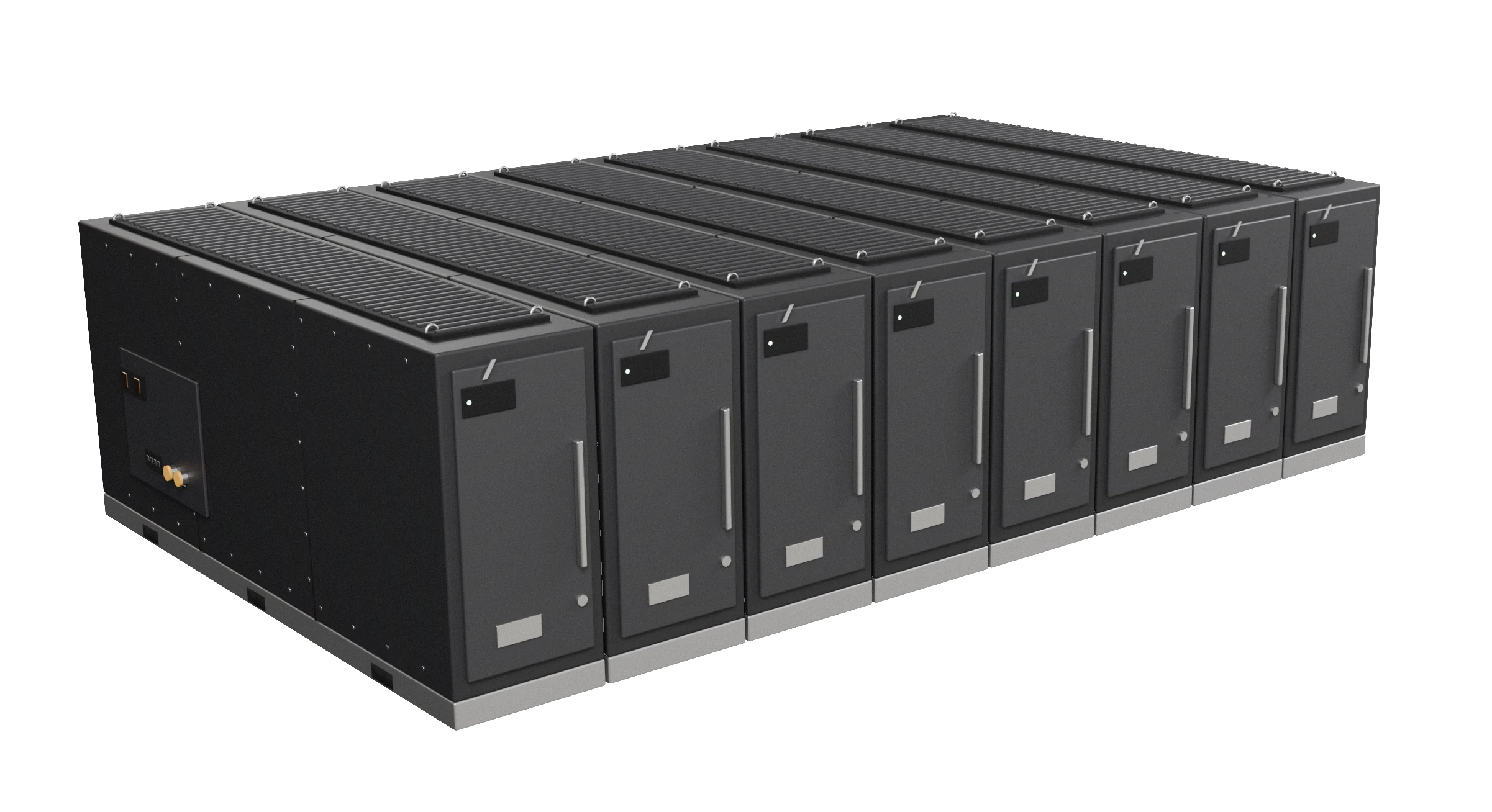
What is inside, and whose it is.
Buy the silicon, own everything above it. For the first generations a cell runs on parts that exist and that we can measure: an AMD Ryzen AI Max+ 395 class part with its 128 GB of unified memory for the decode modules, a discrete GPU for prefill, an ordinary server CPU as host, a 400G switch, a busbar tap instead of a power supply, one liquid loop. What Spliced makes is the module board, the cold plate, the capped clock, the enclosure, the dock, the operating system and the scheduler. That is most of what a cell is.
Our own chip, or not
The measurements say decode wants a small die with as much bandwidth as can be attached, at a fixed low clock, and no vendor sells exactly that. That is a real argument for a chip. Against it, today: the expensive part of an accelerator is the memory stack and the packaging, which we would buy anyway, and a two-person group cannot tape out a die. The test is in our software: once cells are measured, split a token's joules into memory traffic, compute, interconnect and overhead. If compute is a small share, a bought part is already near the roofline. We do not know which yet, and will not say we do.
Spliced Linux
Not a distribution: an appliance image. An upstream kernel with the accelerator drivers we measure with, a read-only root built from a recipe, two slots with signed whole-image updates, one service manager, and one workload, the scheduler. The clock cap is set at boot and verified under load; every cell reports package power, clock and busy for every module, and the number it reports is the number we publish. The first deliverable costs only time: a recipe that boots the machine we own and reproduces our capped figures within 3%.